Aim
Perovskite solar cells have emerged as one of the most promising technologies in photovoltaics, with power conversion efficiencies exceeding 26% in little more than a decade. However, the path to commercialization is hindered by significant challenges. Perovskite materials are notorious for their sensitivity to environmental factors such as moisture, oxygen, and UV light. More critically, surface and interface defects lead to non-radiative recombination, limiting operational stability and theoretical maximum efficiency. Understanding the complex charge carrier dynamics at these interfaces is essential for further optimization.
This study highlights the sensitivity of Surface Photovoltage measurements in evaluating interfacial engineering within perovskite solar cells. By using SPV as a rapid, non-destructive feedback loop, researchers can:
precisely calibrate layer thicknesses and material combinations
accelerates the development of high-efficiency architectures
minimizing material waste and processing time
ultimately paving the way for stable, commercial-grade perovskite photovoltaics.
Application example
Optimizing the C60/SnOx Interface
In collaboration with Fraunhofer ISE, which provided samples and valuable insights into perovskite solar cell processing, the influence of a C60 interlayer on charge‑carrier dynamics was investigated. C60 is widely used as an electron transport layer (ETL) due to its favorable energetic alignment with the perovskite conduction band. It extracts electrons efficiently from the perovskite absorber while blocking holes and protecting the interface. A key objective was to determine the optimal C60 thickness required for efficient electron extraction. Furthermore, an SnOx layer was added for half of the samples, which is known to improve electron extraction and suppressing recombination.

Figure 1: SPV amplitude @2.5 eV of samples with different C60 layer thicknesses, with and without a SnOx layer
Figure 1 shows the SPV amplitude at 2.5 eV (above bandgap) for samples with varying C60 thicknesses, with and without an additional SnOx layer, measured with a low light intensity and long light pulse. No preconditioning was performed. Interestingly, the amplitude reaches its maximum at a thickness of only 3 nm. While literature often recommends at least 20 nm for pinhole‑free coverage, the SPV data indicate that the electronic passivation effect becomes dominant at much lower thicknesses. Furthermore, samples incorporating SnOx exhibit significantly higher amplitudes, confirming that SnOx acts as a good passivation layer.
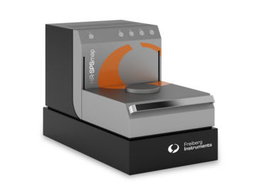
Using the SPSmap with a 660 nm laser diode, rapid 30‑second mappings were performed. Figure 2 compares a sample without C60 or SnOx to the sample showing the highest amplitude (3 nm C60 + SnOx).

No C60, without SnOx

3 nm C60 layer, with SnOx

Figure 2: mappings of the SPV signal amplitude at 660 nm, measured within 30 s; comparison of a sample without C60 and a sample with a 3 nm C60 layer and SnOx
Figure 3 presents spectrally resolved transient SPV contour plots (signal amplitude vs. photon energy over time), measured with a combination of a Kelvin probe for maximum sensitivity with a high‑intensity tunable laser for probing fast processes. Again, a sample without C60/SnOx was compared to one with a 3 nm C60 layer and SnOx. Both samples exhibit significant sub‑bandgap contributions, indicating the presence of defect states that are not fully passivated by C60. However, the sample with C60 and SnOx shows substantially higher above‑bandgap amplitudes, demonstrating improved passivation and more efficient charge extraction.

No C60 layer, no SnOx

3 nm C60 layer and SnOx
Figure 3: comparison of the contour plots measured with a tunable laser of a sample without C60 and a sample with a 15 nm C60 layer
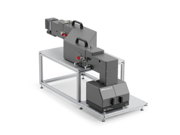
To investigate slower processes, Kelvin probe was combined with the DPM100 monochromator, using an integrated 7 Hz chopper for modulated illumination. Figure 4 shows the resulting contour plots. In the sample without C60, the SPV signal becomes positive after the light is switched off — clear evidence that electrons are not efficiently extracted and that trap‑dominated dynamics are dominant. In contrast, the sample with a C60 layer exhibits a much stronger and consistently negative signal, confirming effective electron extraction.

No C60 layer, no SnOx

3 nm C60 layer and SnOx
Figure 4: comparison of the contour plots measured with the DPM100 of a sample without C60 and a sample with a 15 nm C60 layer
Conclusion
SPV successfully demonstrated that even ultra-thin layers of C60 significantly enhance the electron extraction. Furthermore, the data confirms the synergistic effect of the C60/SnOx bilayer, where SnOx acts as a passivation layer and improves the electron extraction.
Supported by

Acknowledgment: Many thanks to Fraunhofer ISE for providing the samples and valuable insight in Perovskite stacks. This work was performed within the PERLE project funded by the Federal Ministry for Economy Affairs and Energy.