Aim
Semiconductors are the core of modern electronics – but even the smallest local defect can significantly impact their performance and reliability. Spatially resolved defect analysis by lifetime measurements reveals exactly these critical weak points, uncovering insights that other measurement methods often miss.
By examining individual regions of a semiconductor with high precision, you can:
Detect microscopic material defects such as cracks, dislocations, or contamination
Optimize manufacturing processes by pinpointing the root causes of local irregularities
Significantly enhance device lifetime and overall reliability
In a market driven by miniaturization, higher power density, and stringent quality demands, spatially resolved defect analysis provides a decisive competitive advantage. With the MDPmap from Freiberg Instruments it is possible to measure the minority carrier lifetime with high spatial resolution. Taking it one step further, Freiberg Instruments developed an integrated heated sample chuck to perform annealing steps.
Solution
The integrated heating chuck in the MDPmap allows to perform annealing steps in the range of 50 °C up to 250°C without the need to move the sample, thus spatial resolved investigations of the sample can be performed. It was specifically designed to allow samples up to 12’’ diameter.
Furthermore, it is possible to perform sequences in combination with illumination to change the state of defects (e.g. association and dissociation of FeB pairs) and measure and map the lifetime up to 100 °C.
For temperature dependent lifetime measurements in larger temperature ranges for the investigation of activation energies of defects, please have a look at our tools MDpicts, MDpicts pro and HTpicts.
Application example
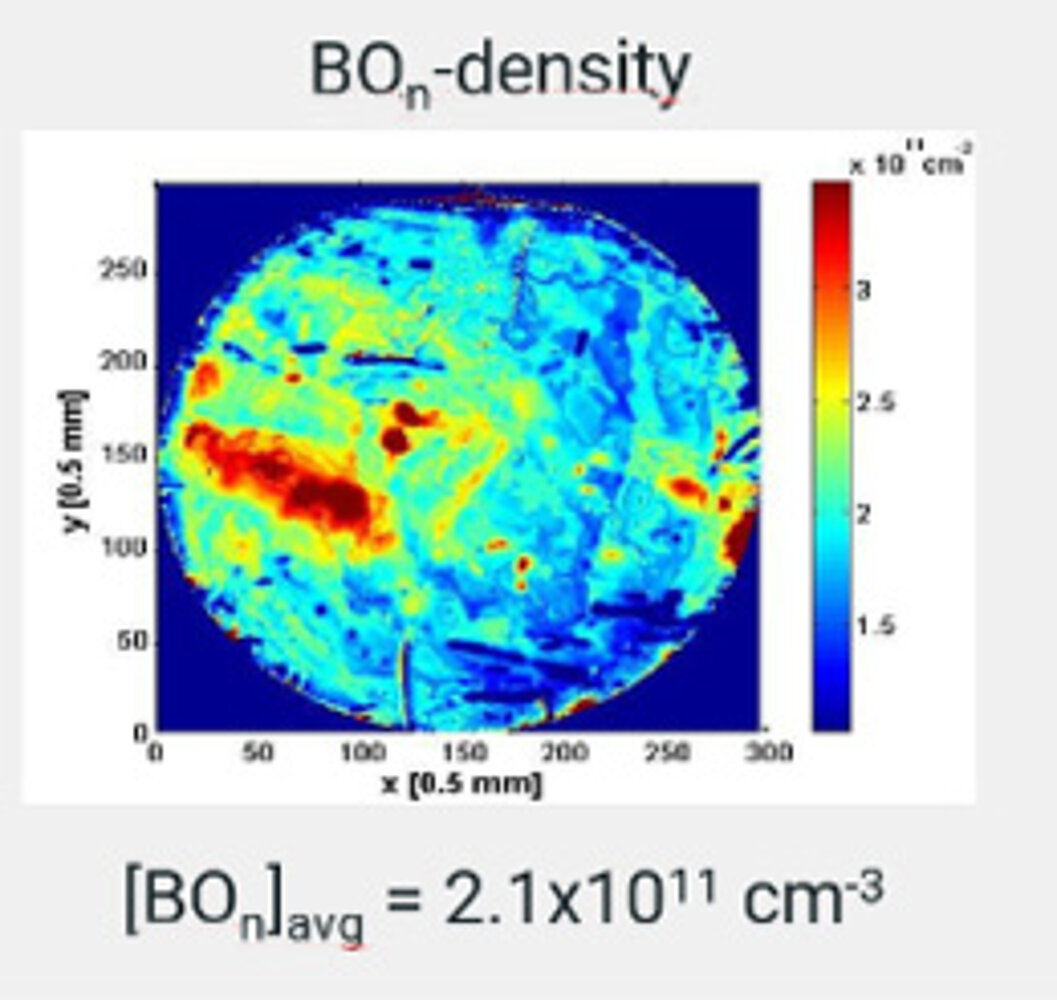
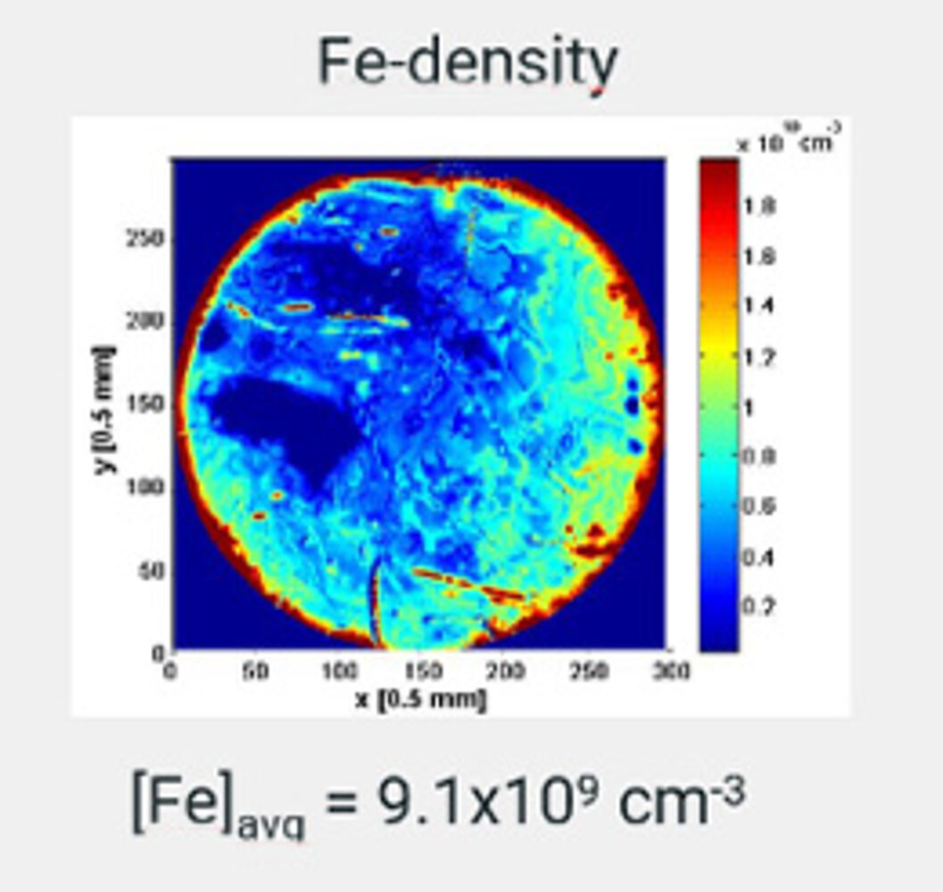
By using the integrated heating stage with a special sequence of annealing steps and light illumination, the concentrations of Chromium, Iron and Boron-Oxgen-Complexes can be determined from lifetime measurements with a detection limit far better than e.g. with chemical methods.
The following steps can be automatically performed with the MDPmap:
Annealing | FeB | CrB | BO2 | Map |
| 30 min at 250 °C | dissociated | dissociated | dissociated | 1 |
| 24 h at 70 °C | associated | associated | dissociated | 2 |
| 30 min at 200 °C | dissociated | associated | dissociated | 3 |
| 10 min at 90 °C | associated | associated | dissociated | 4 |
| Flashing | dissociated | associated | associated | 5 |
| 10 min at 90 °C | associated | associated | associated | 6 |
After each annealing or flashing step a lifetime map is measured. Concentrations of Fe, Cr and BO2 are calculated by usage of following equations:
\([Fe] = C_{Fe} \cdot (\cfrac{1}{\tau_{6}} - \cfrac{1}{\tau_{5}})\) CFe = -2.5 x 10¹³ µscm-3
\([BO_{2}] = C_{BO} \cdot (\cfrac{1}{\tau_{6}} - \cfrac{1}{\tau_{4}})\) CBO = 1.2 x 10¹⁴ µscm-3
\([Cr] = C_{Cr} \cdot (\cfrac{1}{\tau_{1}} - \cfrac{1}{\tau_{3}})\) CCr = 1.6 x 10¹³ µscm-3
The calibration factors are approximations. The accurate values are injection depended and may be calculated by usage of SRH simulations. Nonetheless, the resulting maps show a relative map of the defect densities and hence where defects are concentrated. In the example below iron is concentrated at the edge of the sample, which is typical for Cz-Si, Cr has the highest density at the edge and in circular shaped regions in the center of the sample, whereas BO2 is solely concentrated in large areas in the center of the sample and not at the edge.
In short: When you understand semiconductors locally, you can make better decisions globally.

Related Solutions and Industries: Epitaxial Layers & Thin Films, Photovoltaic
